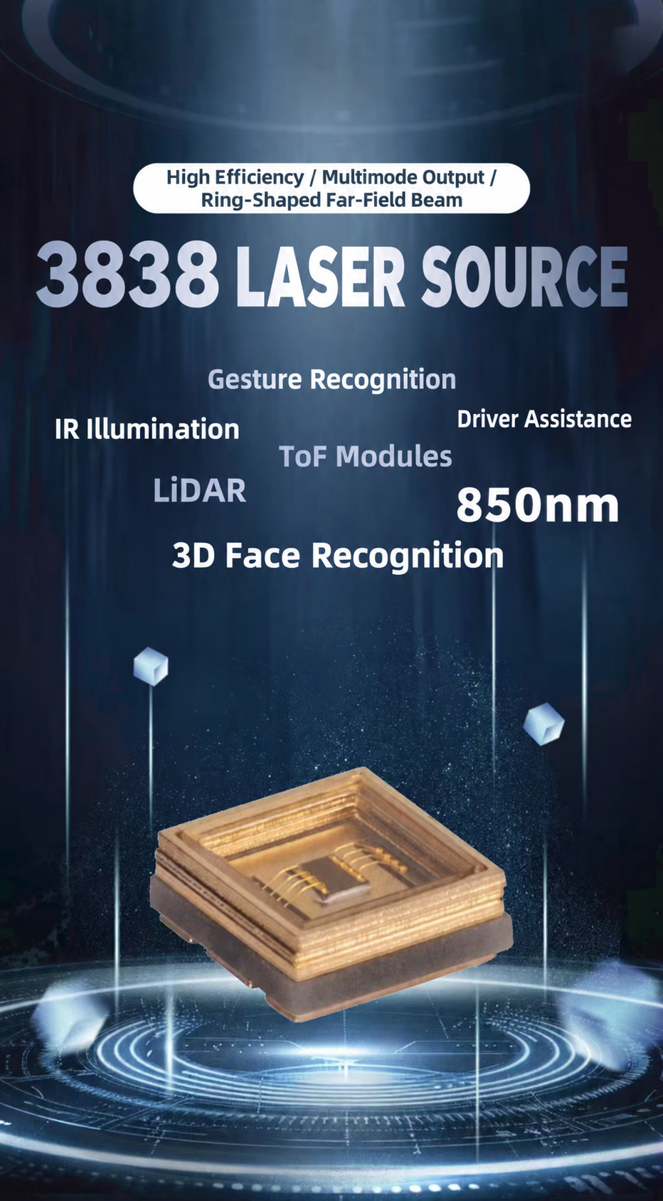
3838
850 nm
Multimode / ring-shaped far-field reference
The supplied material identifies an 850 nm laser source and a ring-shaped far-field beam. Confirm the exact emitter and optics before selection.
View English reference ↗NEAR-INFRARED EMITTERS · CUSTOM MODULE DEVELOPMENT
Develop a VCSEL optical module around your sensing system’s receiver, working distance and illumination field. Review emitter packages, drive waveforms, beam-shaping optics and board formats together, with a defined system-validation and laser-safety scope.
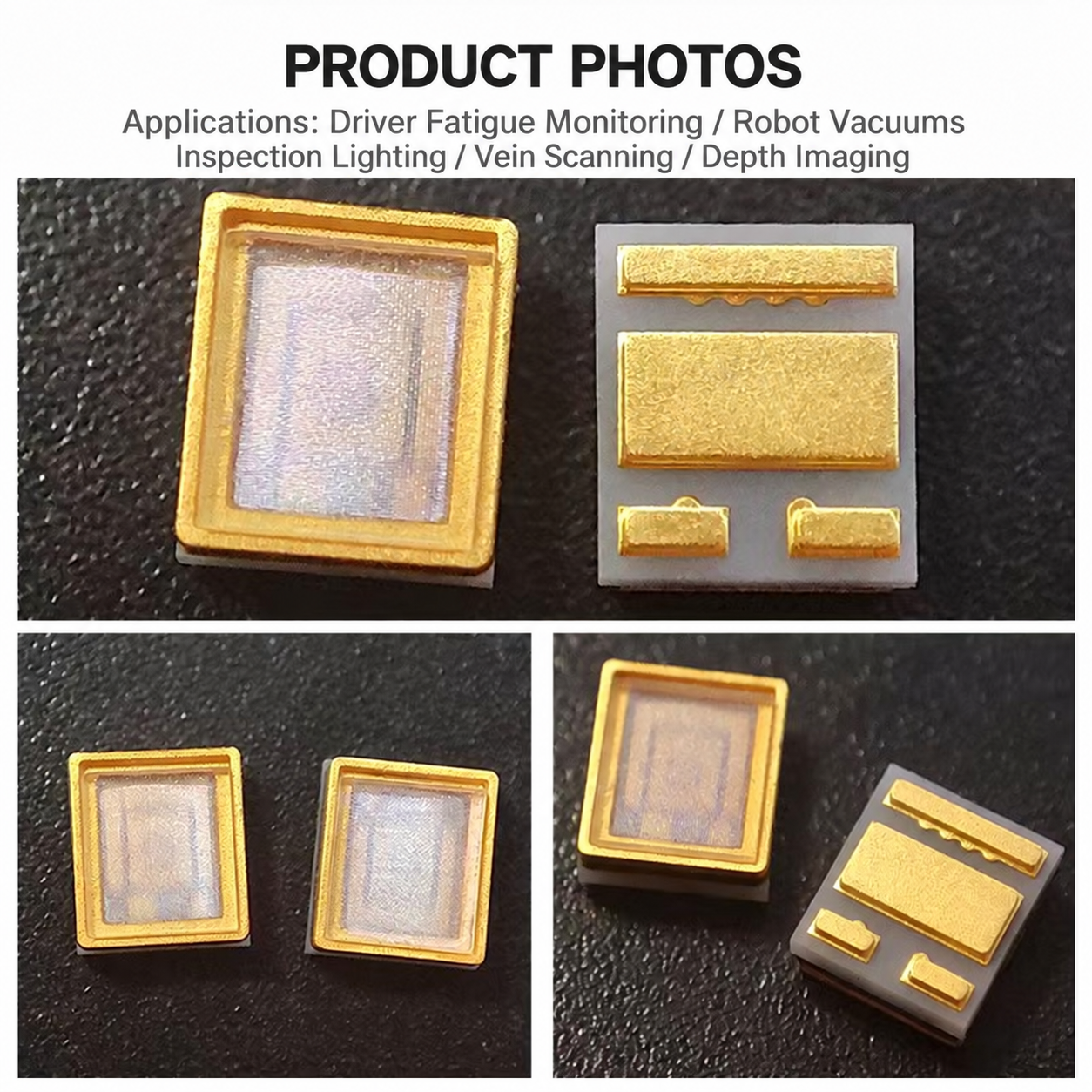
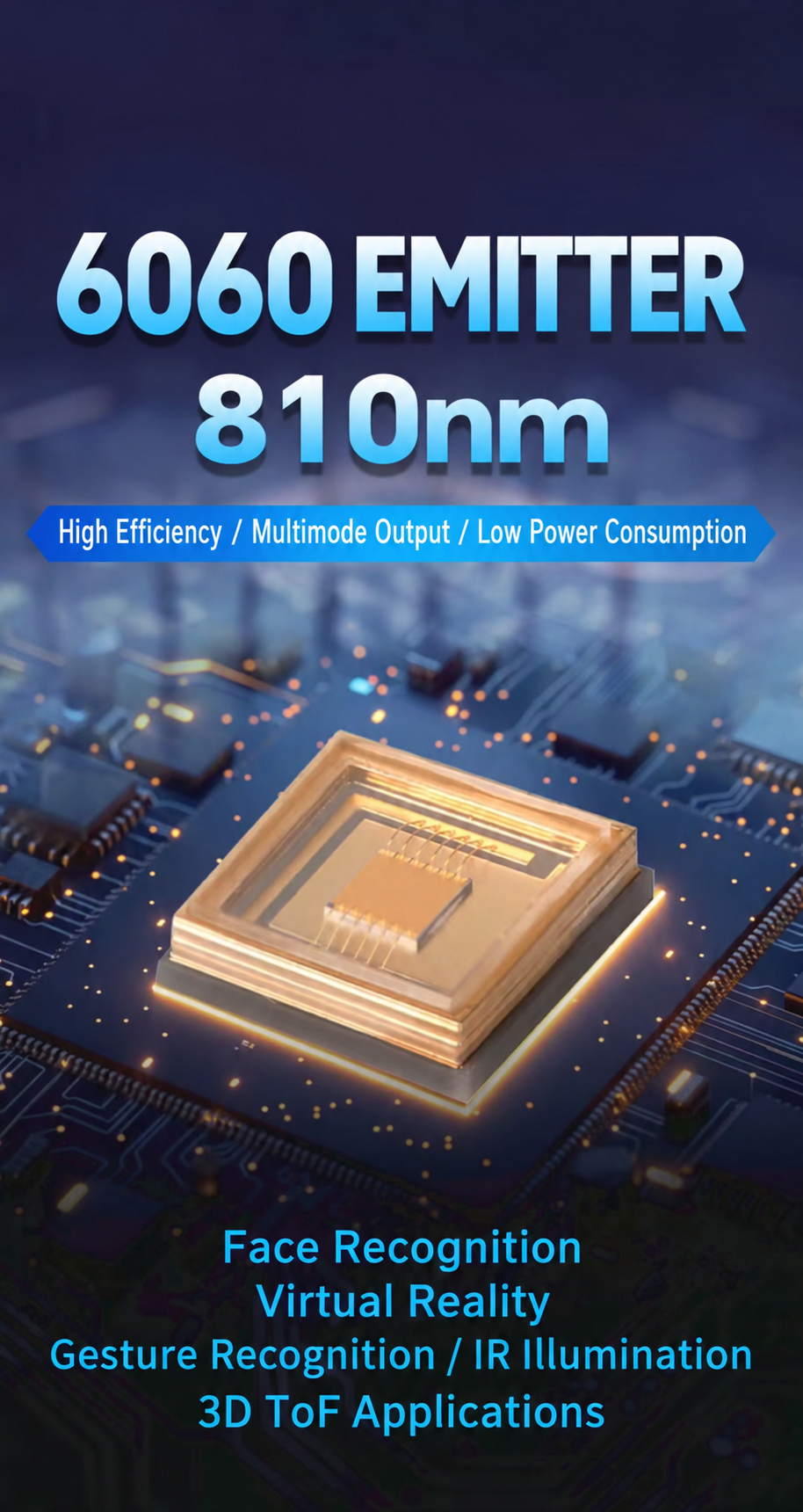
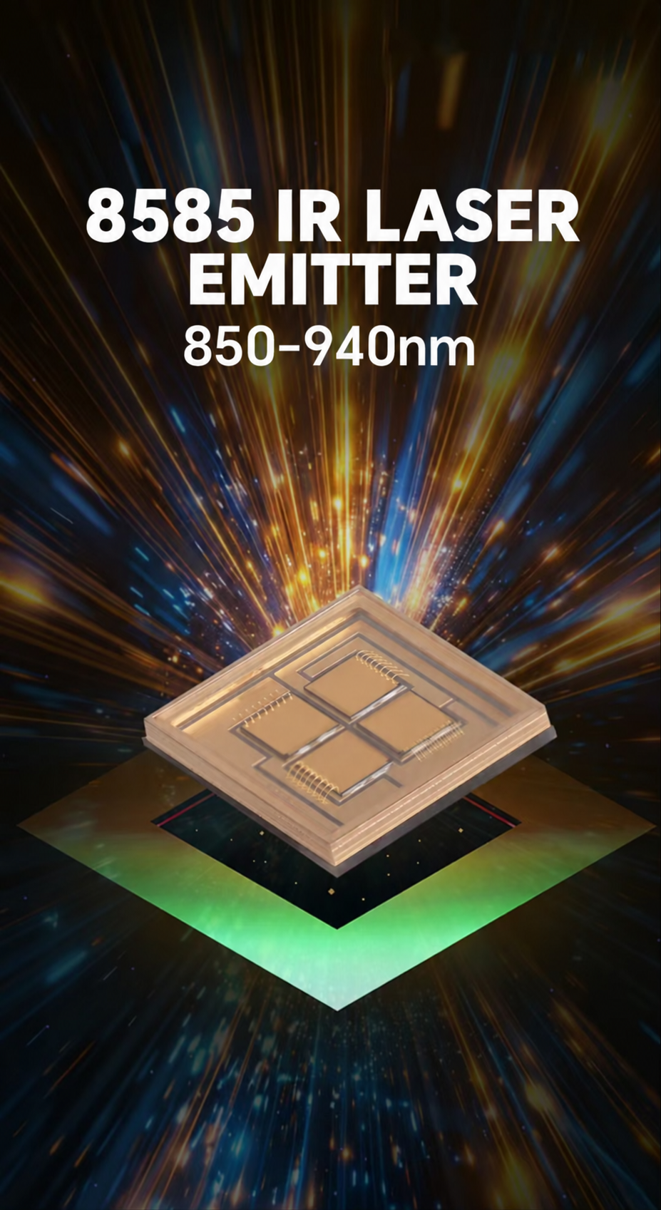
3838 / 6060 / 8585 package references
Wavelength references: 810 nm, 850 nm and 850–940 nm
Emitter arrays, lenses and diffuser evaluation
Review the inputs needed to start
↓APPLICATION FIRST
Start with your receiver, working distance and illuminated area. Review the emitter package, board arrangement, optics and drive conditions together, then define the measurements needed to validate the complete module. The reference families below are starting points for selection, not interchangeable finished products.
01 / EMITTER SELECTION
Compare the labels in the supplied material, then request a part-specific datasheet. Package codes alone do not establish dimensions, pinout, optical power or drive limits.
The supplied material identifies an 850 nm laser source and a ring-shaped far-field beam. Confirm the exact emitter and optics before selection.
View English reference ↗
An 810 nm reference for an infrared illumination brief. Confirm receiver sensitivity, spectral bandwidth and operating conditions for your system.
View English reference ↗
The source labels this family 850–940 nm. Exact available wavelengths and part numbers must be confirmed; this is not a claim of continuous tuning.
View English reference ↗02 / BEAM & DIFFUSER REFERENCES
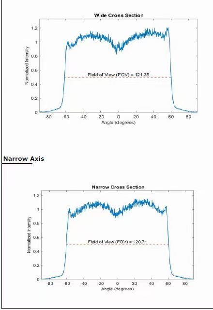
Bring the required field of view, working distance, target-plane uniformity and receiver coverage. Use the original plots below to frame the optics discussion.
The supplied plots label wide-axis FOV 121.35° and narrow-axis FOV 120.71°. These values belong to the reference plot, not to every package or module.
Inspect original plot ↗
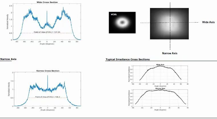
Compare the supplied ring-beam image, cross sections and shaped irradiance example. The material does not identify a matching production part for each profile.
Inspect original plot ↗
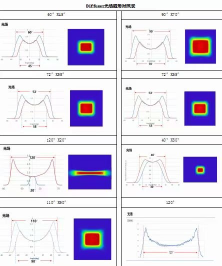
Source examples include 60° × 45°, 90° × 70°, 120° × 20° and 40° × 30°. Use these as discussion targets; compatibility and delivered FOV require optical evaluation.
Inspect original plot ↗Reference images only. The original charts are low-resolution; request full-resolution optical data and test conditions before specifying a beam. Measurement method, source-to-optics pairing and operating conditions must be established for the selected assembly.
03 / MODULE & BENCH REFERENCES
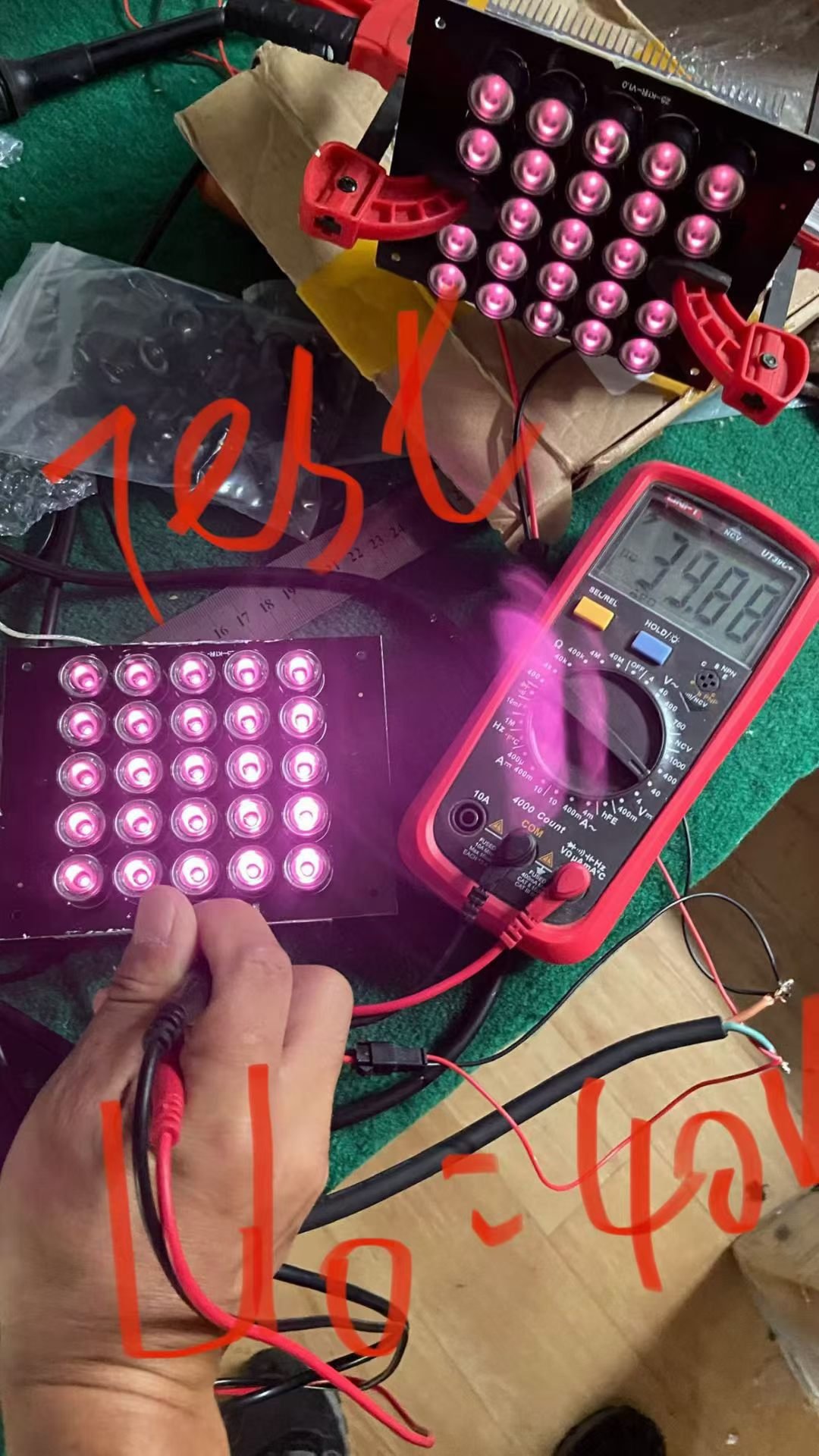
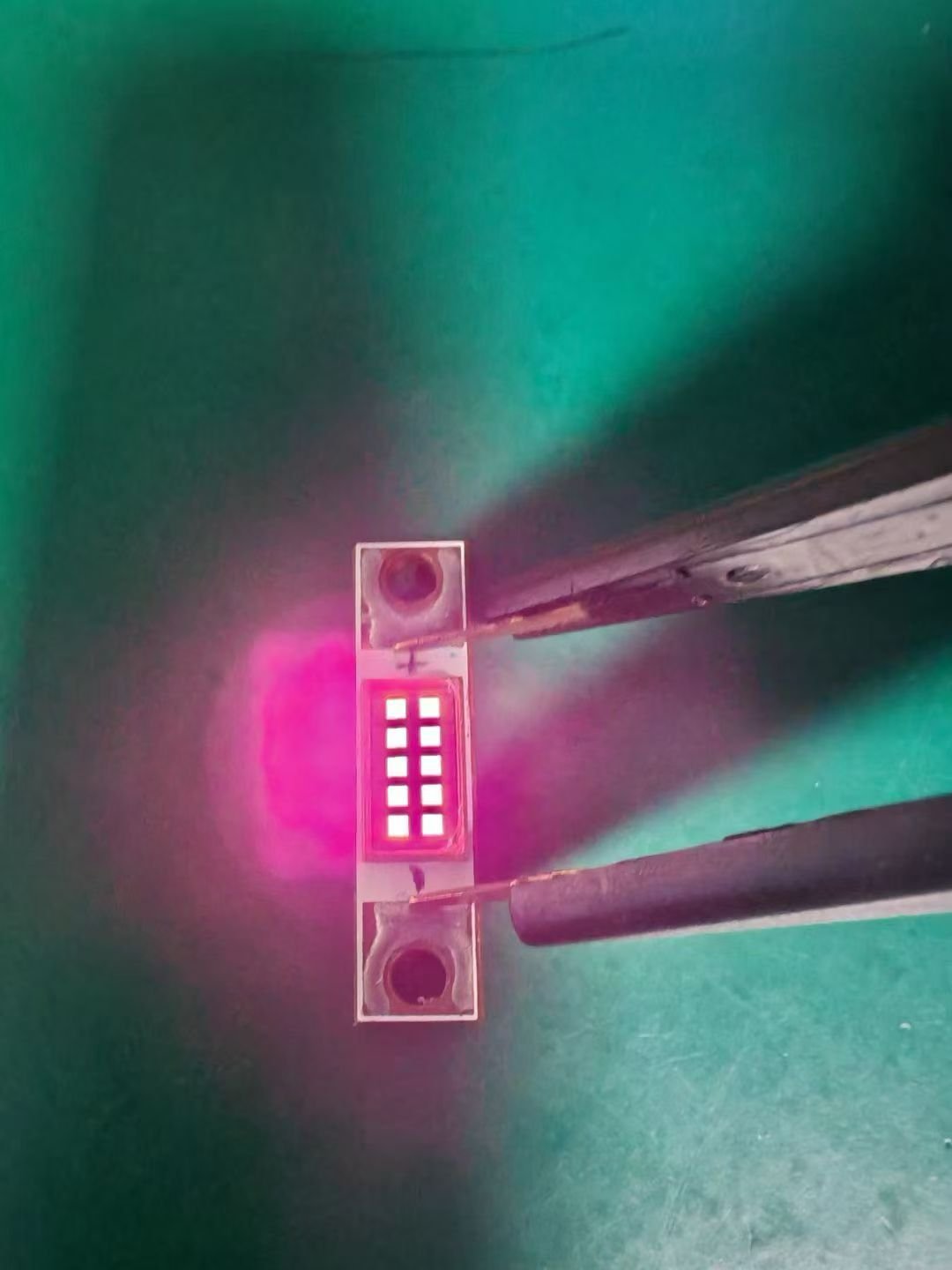
Original photographs show array, lens-equipped and compact linear assembly formats. Each example needs its own emitter identification and electrical, optical and thermal specification.
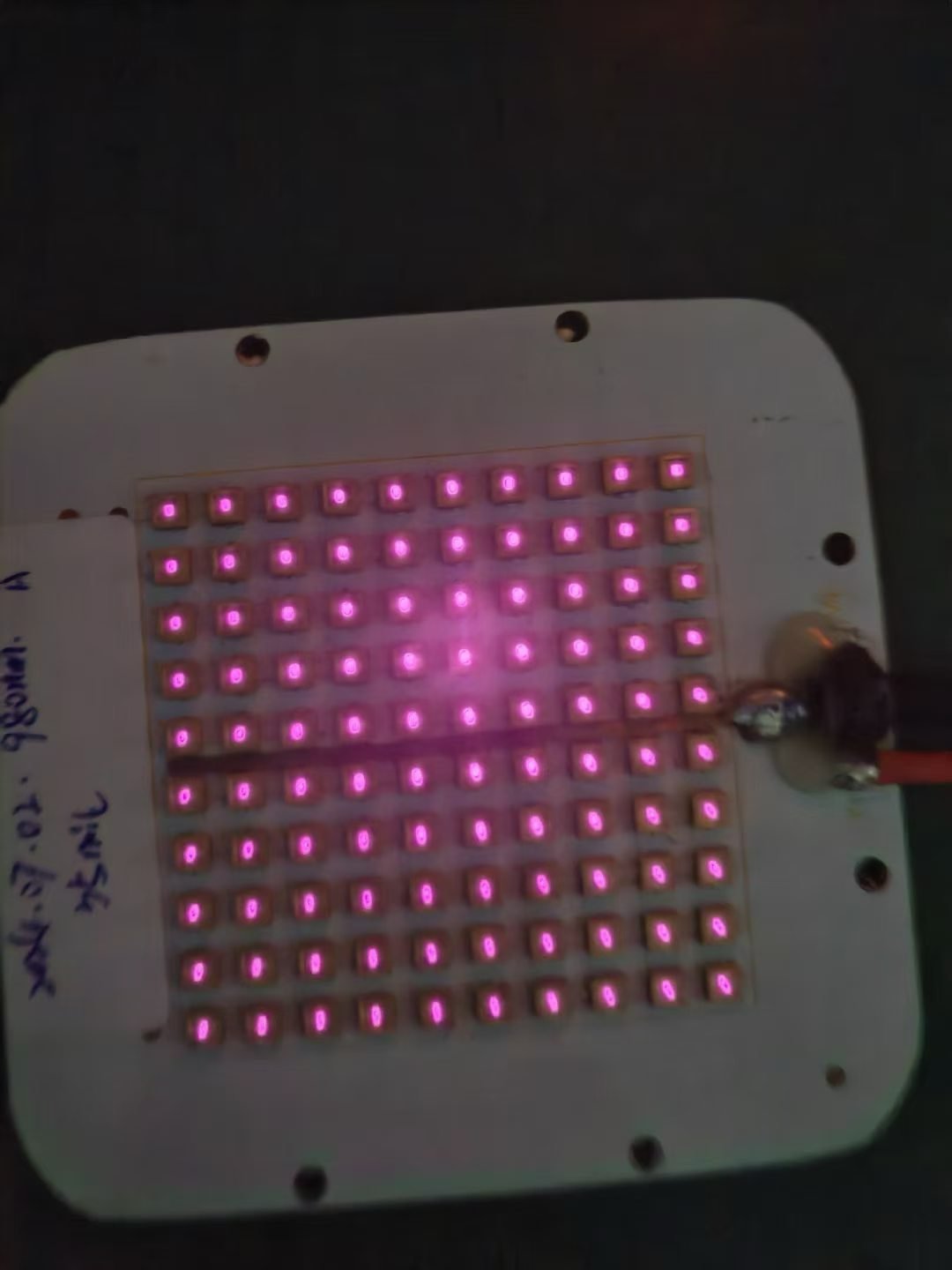
A populated array shown powered on a bench. Discuss coverage, emitter pitch, board outline and the thermal interface for your application.
View full photograph ↗
Original bench photograph of lens-array assemblies and test equipment. Meter readings and handwritten notes are not used as rated product specifications.
View full photograph ↗
A compact emitter arrangement with end connections, shown during a bench test. Mechanical drawings and electrical limits remain part-specific.
View full photograph ↗DEFINE BEFORE DESIGN
Confirmed requirements, preferred targets, and open questions can all be included in the first brief. Unknown values stay visible until they are reviewed.
Wavelength, output definition, beam profile, divergence, field of view, uniformity, working distance, and receiver relationship.
VCSEL part, array arrangement, binning, traceability, series or parallel connections, and supplier data.
Peak and average current, pulse width, repetition rate, duty cycle, rise and fall targets, and synchronization.
Board, copper, heat spreader, thermal interface, enclosure, ambient, duty cycle, temperature sensing, and derating.
Lens, diffuser, window, alignment, tolerance stack, contamination control, mounting, connector, and assembly.
Feedback, interlocks, fault state, calibration, laser classification, accessible emission, test method, and documentation.

PROJECT FIT
Application directions shown in the supplied material. System suitability, sensing accuracy and qualification must be evaluated for the finished product.
Review illumination field, receiver overlap, pulse synchronization and working distance for depth imaging and gesture-recognition systems.
Define the illuminated area, scene contrast, optical filtering and camera timing for inspection equipment or robot sensing.
Evaluate infrared illumination for driver-monitoring systems. Vehicle qualification and system-level performance require separate validation.
Review spectral response and illumination geometry for face or vein imaging. These references do not establish biometric accuracy or medical suitability.
CONTROLLED DEVELOPMENT PATH
A review result, prototype, or sample remains a project stage. Production begins only from the information and acceptance criteria approved for that project.
Confirm geometry, electrical input, optical target, thermal conditions, quantity, and the available source material.
Define the board, emitter arrangement, drive conditions, connections, mounting, and prototype route.
Review the agreed electrical, optical, thermal, mechanical, and safety-related acceptance points.
Carry the confirmed design, BOM, assembly, inspection, labeling, and packing information into production.
DESIGN & MANUFACTURING SUPPORT
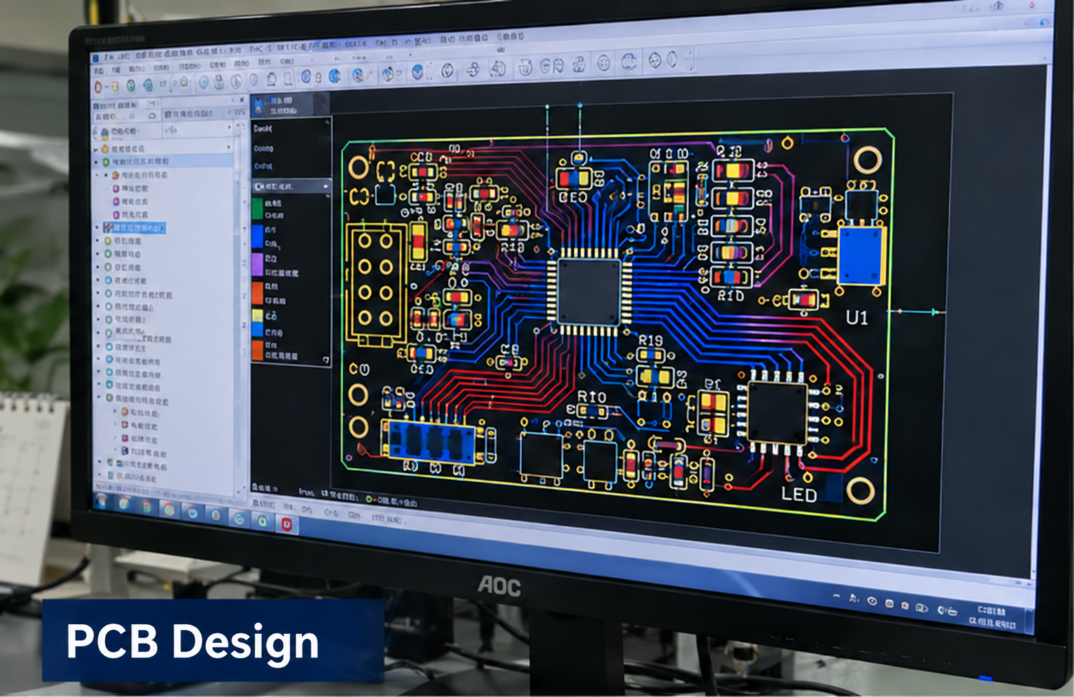
Our in-house PCB design connects your product requirements with manufacturing and testing capabilities at our partner factories.
In-house design
Circuit and PCB layout developed around your product requirements.
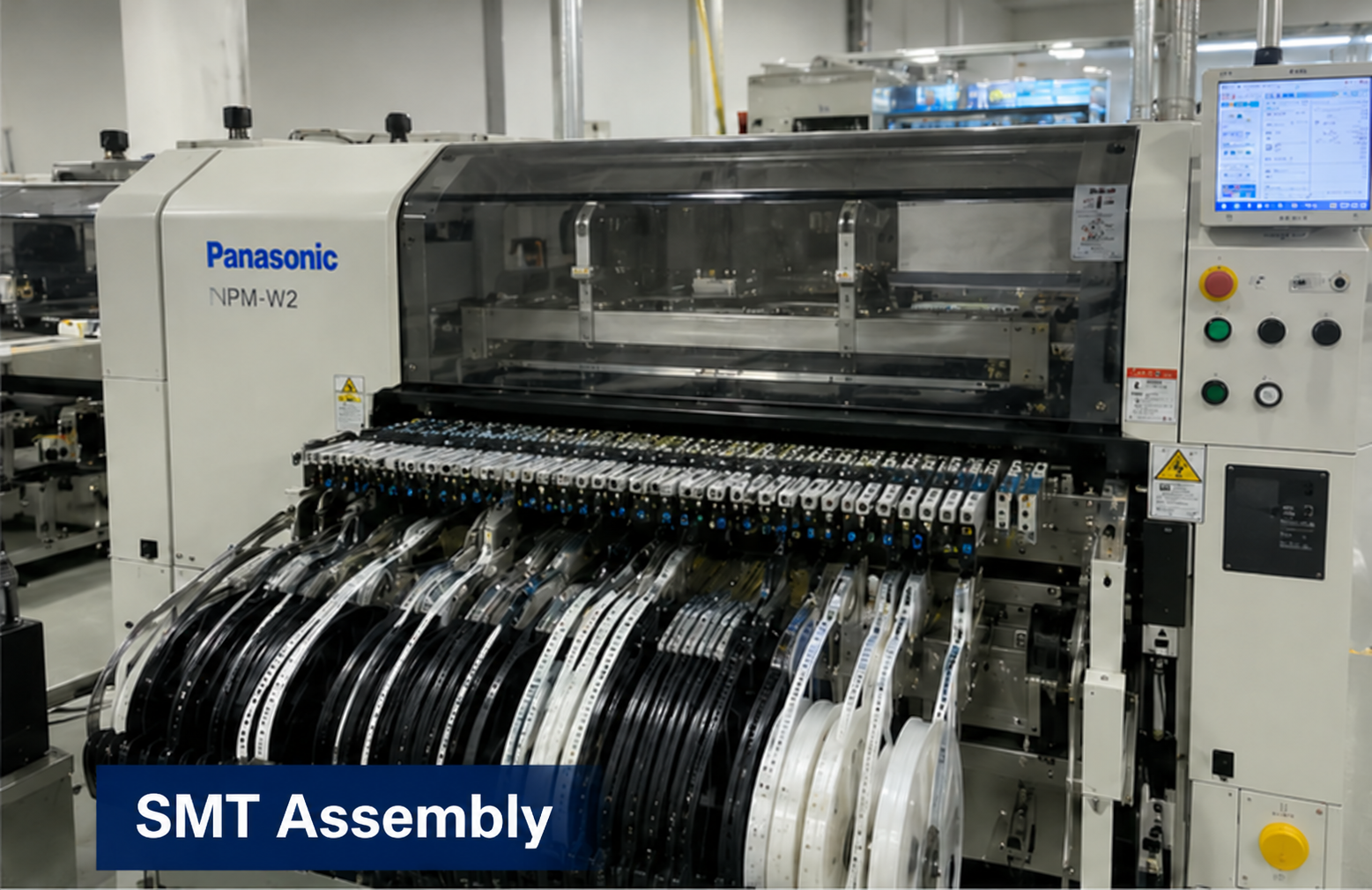
Partner factory
Component placement and assembly for the approved board design.
Partner factory
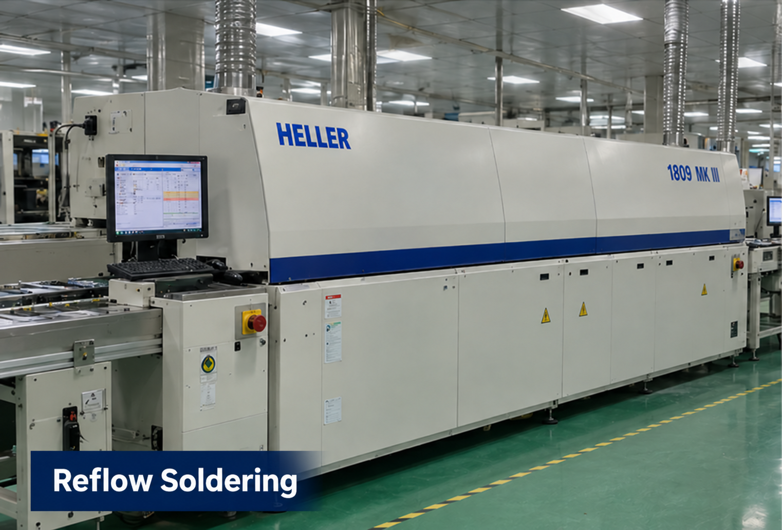
Reflow soldering as part of the board assembly process.
Partner factory
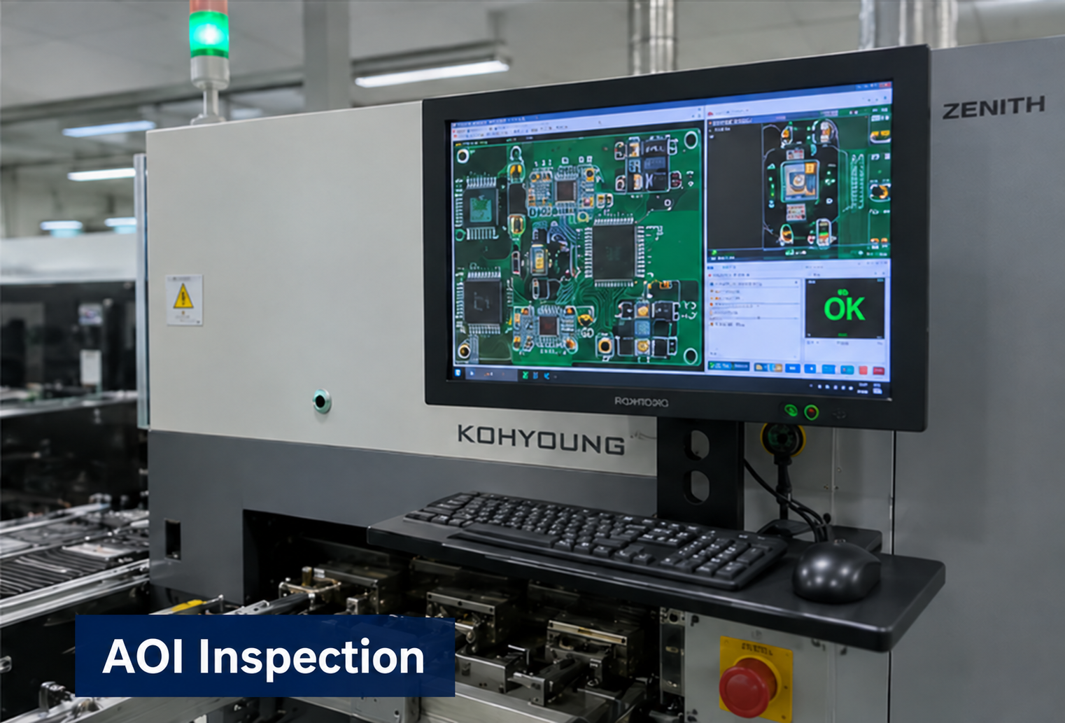
Optical inspection to support assembly quality checks.
Partner factory
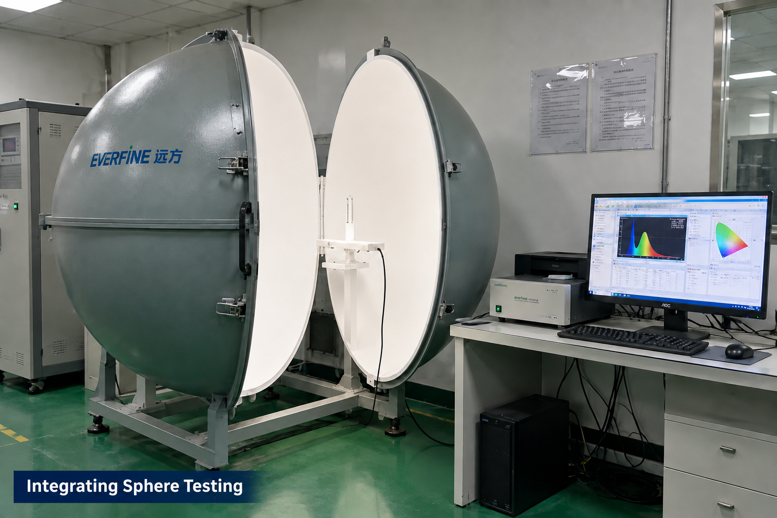
Optical measurement for applicable LED module projects.
Manufacturing and testing scope is agreed for each project. Integrating sphere testing applies to LED optical projects; it is not a required test for every control board. These images illustrate capabilities, not test results or certification for this product.
PROJECT QUESTIONS
These answers describe how a project can begin. They do not promise an unreviewed specification, performance result, certification, schedule, or price.
No. Beam profile, array, drive waveform, pulse timing, duty cycle, temperature, optics, working distance, monitoring, safety, availability, and the receiver or target also matter.
It can be evaluated when peak and average current, pulse width, repetition rate, timing, synchronization, efficiency, thermal, layout, EMI, and safety requirements are defined.
Optics and mechanical alignment can be reviewed with the module, but lens data, tolerances, contamination control, assembly method, calibration, and optical acceptance criteria must be available.
Send the application, wavelength, optical and timing targets, working distance, receiver information, emitter preference, driver conditions, optics, board space, thermal path, interface, quantity, target date, and required validation or laser-safety documents.
PROJECT INQUIRY
Include the application, confirmed inputs, preferred targets, expected quantity, target date, and available drawings, photos, files, or samples.
Inquiry about: VCSEL Optical Modules